The analysis or design of a transistor amplifier requires knowledge of both the dc and
ac response of the system.In fact, the amplifier increases the strength of a weak signal
by transferring the energy from the applied DC source to the weak input ac signal
• The analysis or design of any electronic amplifier therefore has two components:
• The dc portion and
• The ac portion
During the design stage, the choice of parameters for the required dc levels will
affect the ac response.
What is biasing circuit?
• Once the desired dc current and voltage levels have been identified, a network
must be constructed that will establish the desired values of IB, IC and VCE, Such a
network is known as biasing circuit. A biasing network has to preferably make
use of one power supply to bias both the junctions of the transistor.
Purpose of the DC biasing circuit
• To turn the device “ON”
• To place it in operation in the region of its characteristic where the device
operates most linearly, i.e. to set up the initial dc values of IB, IC, and VCE
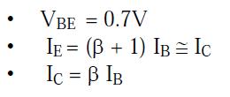
Important basic relationship


0 comments