 RSS
RSS Twitter
 Facebook
Showing posts with label Diode. Show all posts
ANALOG ELECTRONIC CIRCUITS × Diode
Application of diode as Clippers
• Clippers have ability to “clip/remove” off a portion of the input signal without
distorting the remaining part of the alternating waveform.
• HWR is simplest form of clippers. The orientation of diode is going to decide the part
of sinusoidal waveform to be clipped off.
Clipper configuration
Depending on the way in which the diodes are connected with the input, the clipper are
classified in to two major categories, viz.,
• Series configuration
• Parallel configuration
1. Series clipper example 1

1. Series Clipper example 2

1. Series clipper ex – 3 & 4

1. Series clipper Ex - 5 & 6

Various clipepr examples along with transfer characteristics
Biased parallel


ANALOG ELECTRONIC CIRCUITS × Diode
Centre - tap Full-wave Rectifier


• Two diodes and a center-tapped transformer are required.
• VDC = 0.636(Vm)
• Note that Vm here is the transformer secondary voltage to the tap.
Operation
For the positive half of the AC cycle:
For the negative half of the AC cycle:
ANALOG ELECTRONIC CIRCUITS × Diode
Full-wave Rectifiers Bridge

Working :
• For the positive half of the AC cycle:
• Diode D1 and D2 gets forward biased and conducts

Working :
• For the negative half of the AC cycle
• Diode D3 and D4 gets forward biased and conducts during this half cycle.

Details of working of FWR
• We initially consider the diodes to be ideal, such that VC =0 and Rf =0
• The four-diode bridge can be bought as a package During positive half cycles vi is
positive.
• Current is conducted through diodes D1, resistor R and diode D2
• Meanwhile diodes D3 and D4 are reverse biased
• During negative half cycles vi is negative.
• Current is conducted through diodes D3, resistor R and diode D4
• Meanwhile diodes D1 and D2 are reverse biased.
• Current always flows the same way through the load R.

• the average d.c. value of this full-wave-rectified sine wave is VAV = 2VM/p (i.e. twice
the half-wave value)
• Two diodes are in the conduction path.
• Thus in the case of non-ideal diodes vowill be lower than vi by 2VC.
• As for the half-wave rectifier a reservoir capacitor can be used. In the full wave case
the discharge time is T/2 and

ANALOG ELECTRONIC CIRCUITS × Diode

Vdc = 0.318 Vm
If the effect of VT is also
considered, the output of the
system will as below
Vdc = 0.318 (Vm- VT)
Effect of VT on half-wave rectified signal

PIV rating of Half-wave Rectifiers
PIV rating is very important consideration for rectifier circuits
For the half-wave rectifier must be equal or must not exceed the peak value of the applied voltage
· PIV ≥ Vm
This is the voltage rating that must not be exceeded in the reverse bias region
When vin is negative.

Non Ideal Waveform

Half-wave Rectifier
• The total effect of diode on the output signal is given in below

• The average d.c. value of this half-wave-rectified sine wave is

ANALOG ELECTRONIC CIRCUITS × Diode
· In the approximate model of diode, the rav is not used since the value of this rav is
much less than other series elements of the network.
· This model results in less expenditure of time and effort to obtain results.
· Unless otherwise mentioned this approximate model is used hereforth…
Series diode configuration with DC inputs
• When connected to voltage sources in series, the diode is on if the applied voltage is
in the direction of forward-bias and it is greater than the VT of the diode
• When a diode is on, we can use the approximate model for the on state
Series diode configuration

Here, VD = VT, VR = E - VT
ID = IR = VR / R

Here, VD = E, VR = 0, ID = 0
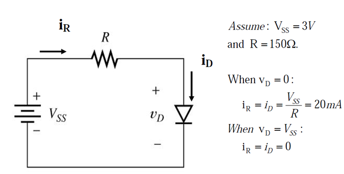
Keep in mind that KVL has to be satisfied under all
Conditions
ANALOG ELECTRONIC CIRCUITS × Diode
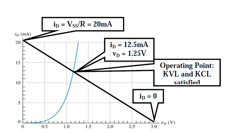
• The applied load will normally have an important impact on region of operation of
device.
• If analysis is done in graphical approach, a line can be drawn on the characteristics of
the device that represents applied load.
• The intersection of load line with the characteristics will determine the point of
operation.
• Such an analysis is called as load-line analysis.
• The intersection point is called ‘Q’ point or operating point.
• Its very simple as compared to the non-linear analysis of diode which involves heavy
maths……

Both KVL and KCL must be satisfied at all times
i-v curves plotted for diode (energised by Vss)

i-v curves plotted for resistor

We can combine these curves on one plot to do a load line analysis
Load line analysis

Example on load line analysis
ANALOG ELECTRONIC CIRCUITS × Diode
• Denoted by trr.
• In FB condition, large number of electrons from n-type progressing through p-type
and large number of holes in p-type is a requirement for conduction. The electrons in
p-type and holes progressing through n-type establish a large number of minority
carriers in each material.
• Now if the diode is changed from FB to RB
• The diode will not instantaneously react to this sudden change. Because of the large
number of minority carriers in each material, the current sustains in diode for a time ts
storage time which is required for minority carriers to return to their majority carrier
state in the opposite material.
• Eventually current will reduce to non conduction levels.
• This time is tt transition interval
• Hence trr= ts + tt
• This is very important consideration in high frequency operation.
• Commercially available diodes have reverse recovery time of few nano seconds to
1micro second.


ANALOG ELECTRONIC CIRCUITS × Diode

• The figure shows the capacitance v/s applied voltage across the diode.
• Shunt capacitive effects that can be ignored at very lower frequencies since Xc=1/2πfc
is very large (open circuit)
• However this can not be neglected in very high frequencies since it introduces a low
reactance (shorting) path.
• Two types of capacitive effects to be considered in FB and RB condition.
• In RB region transition or depletion region capacitance CT in FB diffusion
capacitance CD or storage capacitance.
• W.k.t C=εA/d.
• ε is the permittivity of dielectric between tow plates of area A separated by distance d.
• In RB, depletion region which is free of carriers that behaves essentially like an
insulator between the layers of opposite charges. This depletion region width increase
with increase in RB potential.
• Since d is increasing, capacitance effect is more in FB.
ANALOG ELECTRONIC CIRCUITS × Diode
• An equivalent circuit is a combination of elements properly chosen to best represent
the actual terminal characteristics of a device, system or such a particular operating
region.
• Then device symbol can be replaced with the equivalent circuit which makes the
analysis of the circuit easy and straight forward.
Piece wise linear equivalent circuit

One technique for obtaining equivalent circuit is to approximate the characteristics of the
device by straight line segments
• Rd defines the resistance level of the device when it is in the ON state.
• Ideal diode is included to establish that there is only one direction of conduction
through the device.
• Since silicon semiconductor diode does not conduct until VD of 0.7V is reached, a
battery opposing the conduction direction is included.
Simplified equivalent circuit
• In most of the applications, resistance rav is very small in comparison to the other
elements of the network.
• Removal of this rav from the network makes a simplified equivalent circuit.
• And an ideal diode will start conduction for zero applied voltage.
ANALOG ELECTRONIC CIRCUITS × Diode
Forward Bias region:
• The resistance depends on the amount of current (ID) in the diode.
Rd=Δvd/ ΔId
• The resistance depends on the amount of current (ID) in the diode.
• The voltage across the diode is fairly constant (VT = 26mV for 25°C).
• Reverse Bias region:
Rd=∞
The resistance is essentially infinite. The diode acts like an open.
ANALOG ELECTRONIC CIRCUITS × Diode

Rac=ΔVd/ΔId Point to point
ANALOG ELECTRONIC CIRCUITS × Diode

RD=VD / ID
DC or static resistance
• For a specific applied DC voltage VD, the diode will have a specific current ID,
and a specific resistance RD.
• The amount of resistance RD, depends on the applied DC voltage.
ANALOG ELECTRONIC CIRCUITS × Diode

• As temperature increases it adds energy to the diode.
• It reduces the required Forward bias voltage in Forward Bias condition
• It increases the amount of Reverse current in Reverse Bias condition
• It increases maximum Reverse Bias Avalanche Voltage
• Germanium diodes are more sensitive to temperature variations than Silicon Diodes.
Resistance Levels
• Semiconductors act differently to DC and AC currents.
There are 3 types of resistances.
• DC or Static Resistance
• AC or Dynamic Resistance
• Average AC Resistance
ANALOG ELECTRONIC CIRCUITS × Diode
Breakdown occurs with heavily doped junction regions (ie. highly doped regions are better conductors). If a reverse voltage is applied and the depletion region is too narrow for avalanche breakdown (minority carriers cannot reach high enough energies over the distance traveled ) the electric field will grow. However, electrons are pulled directly from the valence band on the P side to the conduction band on the N side. This type of breakdown is not destructive if the reverse current is limited.
ANALOG ELECTRONIC CIRCUITS × Diode
Avalanche breakdown occurs when a high reverse voltage is applied to a diode and large
electric field is created across the depletion region. The effect is dependant on the doping
levels in the region of the depletion layer. Minority carriers in the depletion region
associated with small leakage currents are accelerated by the field to high enough energies
so that they ionise silicon atoms when they collide with them. A new hole-electron pair are
created which accelerate in opposite directions causing further collisions and ionisation and
avalanche breakdown
ANALOG ELECTRONIC CIRCUITS × Diode
• No Bias
• Forward Bias
• Reverse Bias
No bias condition
• No external voltage is applied: VD = 0V and no current is flowing ID = 0A.

Only a modest depletion layer exists
Reverse bias condition
External voltage is applied across the p-n junction in the opposite polarity of the p- and ntype
materials.

• This causes the depletion layer to widen.
• The electrons in the n-type material are attracted towards the positive terminal and the
‘holes’ in the p-type material are attracted towards the negative terminal.
Forward Bias Condition
• External voltage is applied across the p-n junction in the same polarity of the p- and ntype
materials.
• The depletion layer is narrow.
• The electrons from the n-type material and ‘holes’ from the p-type material have
sufficient energy to cross the junction.
• Actual v-i characteristics is as shown in fig below

ANALOG ELECTRONIC CIRCUITS × Diode

Fig – a semiconductor diode symbol
Basic operation

Fig – b Vi characteristics of a diode
n-type versus p-type
• n-type materials make the Silicon (or Germanium) atoms more negative.
• p-type materials make the Silicon (or Germanium) atoms more positive.
• Join n-type and p-type doped Silicon (or Germanium) to form a p-n junction.
p-n junction
• When the materials are joined, the negatively charged atoms of the n-type doped side
are attracted to the positively charged atoms of the p-type doped side.
• The electrons in the n-type material migrate across the junction to the p-type material
(electron flow).
• the ‘holes’ in the p-type material migrate across the junction to the n-type material
(conventional current flow).
• The result is the formation of a depletion layer around the junction.

Depletion region


