 RSS
RSS Twitter
 Facebook
Showing posts with label Transistor Biasing. Show all posts
ANALOG ELECTRONIC CIRCUITS × Transistor Biasing
Through proper design transistors can be used as switches for computer and control
applications.
When the input voltage VB is high ( logic 1), the transistor is in saturation ( ON). And
the output at its collector = VCE is almost 0V( Logic 0)
Transistor as a switch
When the base voltage VB is low( logic 0), i.e, 0V, the transistor is cutoff( Off) and IC
is 0, drop across RC is 0 and therefore voltage at the collector is VCC.( logic 1)
Thus transistor switch operates as an inverter.
This circuit does not require any DC bias at the base of the transistor.
Design
When Vi ( VB) is 5V, transistor is in saturation and ICsat
Just before saturation, IB,max = IC,sat /βDC
Thus the base current must be greater than IB,max to make the transistor to work in
saturation.
Analysis

When Vi = 5V, the resulting level of IB is
IB = (Vi – 0.7) / RB
= ( 5 – 0.7) / 68k
= 63μA
ICsat = VCC / RC = 5/0.82k
= 6.1mA
Verification
( IC,sat / β) = 48.8μA
Thus IB > ( IC,sat / β) which is required for a transistor to be in saturation.
A transistor can be replaced by a low resistance Rsat when in saturation ( switch on)
Rsat = VCE sat/ ICsat (VCE sat is very small and ICsat is IC,max is maximum current)
A transistor can be replaced by a high resistance Rcutoff when in cutoff ( switch on)
ANALOG ELECTRONIC CIRCUITS × Transistor Biasing

Input loop

Applying KVL for Input Loop:
VCC = IC1RC + IBRB + VBE + IERE
Substituting for IE as (β+1)IB and solving for IB,
IB = ( VCC – VBE) / [ RB + β( RC + RE)]
Output loop

Neglecting the base current, KVL to the output loop results in,
VCE = VCC – IC ( RC + RE)
DC bias with voltage feedback

Input loop

Applying KVL to input loop:
VCC = IC|RC + IBRB + VBE + IERE
IC|~- IC and IC ~= IE
Substituting for IE as (β +1)IB [ or as βIB] and solving for IB,
IB = ( VCC – VBE) / [ RB + β( RC + RE)]
Output loop

Neglecting the base current, and applying KVL to the output loop results in,
VCE = VCC – IC ( RC + RE)
In this circuit, improved stability is obtained by introducing a feedback path from
collector to base.
Sensitivity of Q point to changes in beta or temperature variations is normally less than
that encountered for the fixed bias or emitter biased configurations.
ANALOG ELECTRONIC CIRCUITS × Transistor Biasing

This is the biasing circuit wherein, ICQ and VCEQ are almost independent of β.
The level of IBQ will change with β so as to maintain the values of ICQ and VCEQ almost
same, thus maintaining the stability of Q point.
Two methods of analyzing a voltage divider bias circuit are:
Exact method – can be applied to any voltage divider circuit
Approximate method – direct method, saves time and energy, can be applied in most of
the circuits.
Exact method
In this method, the Thevenin equivalent network for the network to the left of the base
terminal to be found.

To find Rth:

From the above circuit,
Rth = R1|| R2
= R1 R2 / (R1 + R2)
11
To find Eth

From the above circuit,
Eth = VR2 = R2VCC / (R1 + R2)

In the above network, applying KVL
( Eth – VBE) = IB [ Rth +( β + 1) RE ]
IB = ( Eth – VBE) / [ Rth +( β + 1) RE ]
Analysis of Output loop
KVL to the output loop:
VCC = ICRC + VCE + IERE
IE ~= IC
Thus, VCE = VCC – IC (RC + RE)
Note that this is similar to emitter bias circuit.
ANALOG ELECTRONIC CIRCUITS × Transistor Biasing
• It can be shown that, including an emitter resistor in the fixed bias circuit
improves the stability of Q point.
• Thus emitter bias is a biasing circuit very similar to fixed bias circuit with an
emitter resistor added to it.

Input loop
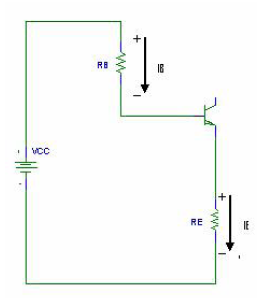
• Writing KVL around the input loop we get,
VCC = IBRB + VBE + IERE (1)
We know that,
IE = (β+1)IB (2)
Substituting this in (1), we get,
VCC = IBRB + VBE + (β+1)IBRE
VCC – VBE = IB(RB + (β+1) RE)
Solving for IB:
IB = (VCC – VBE ) /[(RB + (β+1) RE)]
7
The expression for IB in a fixed bias circuit was,
IB = (VCC – VBE ) /RB
Equivalent input loop:

• REI in the above circuit is (β+1)RE which means that, the emitter resistance that is
common to both the loops appears as such a high resistance in the input loop.
• Thus Ri = (β+1)RE ( more about this when we take up ac analysis)
Output loop

Collector – emitter loop
Applying KVL,
VCC = ICRC + VCE + IERE
IC is almost same as IE
8
Thus,
VCC = ICRC + VCE + ICRE
= IC (RC + RE) +VCE
VCE = VCC - IC (RC + RE)
Since emitter is not connected directly to ground, it is at a potential VE, given by,
VE = IERE
VC = VCE + VE OR VC = VCC – ICRC
Also, VB = VCC – IBRB OR VB = VBE + VE
ANALOG ELECTRONIC CIRCUITS × Transistor Biasing

• The simplest transistor dc bias configuration.
• For dc analysis, open all the capacitance.
DC Analysis
• Applying KVL to the input loop:
VCC = IBRB + VBE
• From the above equation, deriving for IB, we get,
IB = [VCC – VBE] / RB
• The selection of RB sets the level of base current for the operating point.
• Applying KVL for the output loop:
VCC = ICRC + VCE
• Thus,
VCE = VCC – ICRC
4
• In circuits where emitter is grounded,
VCE = VE
VBE = VB
Design and Analysis
• Design: Given – IB, IC , VCE and VCC, or IC , VCE and β , design the values of RB,
RC using the equations obtained by applying KVL to input and output loops.
• Analysis: Given the circuit values (VCC, RB and RC), determine the values of IB,
IC , VCE using the equations obtained by applying KVL to input and output loops.
Problem – Analysis
Given the fixed bias circuit with VCC = 12V, RB = 240 kΩ, RC = 2.2 kΩ and β = 75.
Determine the values of operating point.
Equation for the input loop is:
IB = [VCC – VBE] / RB where VBE = 0.7V,
thus substituting the other given values in the equation, we get
IB = 47.08uA
IC = βIB = 3.53mA
VCE = VCC – ICRC = 4.23V
• When the transistor is biased such that IB is very high so as to make IC very high
such that ICRC drop is almost VCC and VCE is almost 0, the transistor is said to be
in saturation.
IC sat = VCC / RC in a fixed bias circuit.
Verification
• Whenever a fixed bias circuit is analyzed, the value of ICQ obtained could be
verified with the value of ICSat ( = VCC / RC) to understand whether the transistor is
in active region.
• In active region,
ICQ = ( ICSat /2)
Load line analysis
A fixed bias circuit with given values of VCC, RC and RB can be analyzed ( means,
determining the values of IBQ, ICQ and VCEQ) using the concept of load line also.
Here the input loop KVL equation is not used for the purpose of analysis, instead, the
output characteristics of the transistor used in the given circuit and output loop KVL
equation are made use of.
5
• The method of load line analysis is as below:
1. Consider the equation VCE = VCC – ICRC This relates VCE and IC for the given IB
and RC
2. Also, we know that, VCE and IC are related through output characteristics
We know that the equation,
VCE = VCC – ICRC
represents a straight line which can be plotted on the output characteristics of the
transistor.
Such line drawn as per the above equation is known as load line, the slope of which is
decided by the value of RC ( the load).
Load line

• The two extreme points on the load line can be calculated and by joining which
the load line can be drawn.
• To find extreme points, first, Ic is made 0 in the equation: VCE = VCC – ICRC .
This gives the coordinates (VCC,0) on the x axis of the output characteristics.
• The other extreme point is on the y-axis and can be calculated by making VCE = 0
in the equation VCE = VCC – ICRC which gives IC( max) = VCC / RC thus giving the
coordinates of the point as (0, VCC / RC).
• The two extreme points so obtained are joined to form the load line.
• The load line intersects the output characteristics at various points corresponding
to different IBs. The actual operating point is established for the given IB.
Q point variation
As IB is varied, the Q point shifts accordingly on the load line either up or down
depending on IB increased or decreased respectively.
As RC is varied, the Q point shifts to left or right along the same IB line since the
slope of the line varies. As RC increases, slope reduces ( slope is -1/RC) which
results in shift of Q point to the left meaning no variation in IC and reduction in VCE .
Thus if the output characteristics is known, the analysis of the given fixed bias circuit
or designing a fixed bias circuit is possible using load line analysis as mentioned
above.
ANALOG ELECTRONIC CIRCUITS × Transistor Biasing
The analysis or design of a transistor amplifier requires knowledge of both the dc and
ac response of the system.In fact, the amplifier increases the strength of a weak signal
by transferring the energy from the applied DC source to the weak input ac signal
• The analysis or design of any electronic amplifier therefore has two components:
• The dc portion and
• The ac portion
During the design stage, the choice of parameters for the required dc levels will
affect the ac response.
What is biasing circuit?
• Once the desired dc current and voltage levels have been identified, a network
must be constructed that will establish the desired values of IB, IC and VCE, Such a
network is known as biasing circuit. A biasing network has to preferably make
use of one power supply to bias both the junctions of the transistor.
Purpose of the DC biasing circuit
• To turn the device “ON”
• To place it in operation in the region of its characteristic where the device
operates most linearly, i.e. to set up the initial dc values of IB, IC, and VCE
Important basic relationship
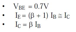
ANALOG ELECTRONIC CIRCUITS × Transistor Biasing

• The values of the parameters IB, IC and VCE together are termed as ‘operating
point’ or Q ( Quiescent) point of the transistor.
Q-Point
• The intersection of the dc bias value of IB with the dc load line determines the Qpoint.
• It is desirable to have the Q-point centered on the load line. Why?
• When a circuit is designed to have a centered Q-point, the amplifier is said to be
midpoint biased.
• Midpoint biasing allows optimum ac operation of the amplifier.
ANALOG ELECTRONIC CIRCUITS × Transistor Biasing
Three operating regions
• Linear – region operation:
– Base – emitter junction forward biased
– Base – collector junction reverse biased
• Cutoff – region operation:
– Base – emitter junction reverse biased
– Base – collector junction reverse biased
• Saturation – region operation:
– Base – emitter junction forward biased
– Base – collector junction forward biased
Three operating regions of BJT


